A single-push reset circuit for STM32
The STM32 family of microcontrollers offers a wide good variety of options when it comes to boot selection. The majority of STM32 devices are flashed at factory with a bootloader that is very permissive and complete; it allows for a wide variety of options when it comes to booting options, boot behaviors, in-system programming through I2C, SPI, serial communication and very good debug features.
One of the most interesting aspects of working with these devices is the way STM tackled the boot selection process, that is, what portion of the memory is used for the stack pointer start. In STM32F0xx devices, there are basically four ways you can boot the MCU: main flash memory, main system memory, embedded SRAM memory, and an “empty check” option only available to STM32F04x and STM32F09x devices.
Despite this page being written for the STM32F072 MCU that I use mainly in my boards, the principles, calculations and simulations are very device-agnostic in the sense that they should work for any STM32F0xx device with some mild adaptation or none at all.
In this article I will detail the many possibilities there are for handling these boot options, and the design of a reset circuit that can reset the MCU simply or drive it to bootloader, using a single push button.
(1) Introduction
Embedded Engineering is fairly complicated shenanigans. It involved dominating technologies and procedures so complex that they need higher education to be fully mastered, and then make those very same technologies and procedures available and accessible to the general public which is very unkowledgeable about technology. Customers generally want a very simple solution to a very complex problem and, sometimes, the best product does not always win if it is not user-friendly – Apple products being the master example for me, being much less powerful than the competitors in the same price range but light-years ahead in terms of user experience and usability.
One of such problems is handling the reset event in an MCU. A microcontroller generally has several memory options, all of which can be invoked, operated, written and erased at runtime and all of which containing their particular use and place. From and end user’s perspective, we want it to just work, but that’s not how it goes in research and development. R&D is a very nonlinear process that requires full mastery of the system being worked on, which is again completely incompatible with user experience due to the general unkowledgeability of the end user.
With the recent addition of ARM processor support to QMK – STM32F103, STM32F072 and STM32F303 – the issue of MCU boot select and how to make it accessible to the end consumer is not yet well understood by the PCB designers of the Custom Mechanical Keyboard community. When ATMEGA processors are concerned, there are very clear and standardized ways we deal with the reset problem.
In this article I will detail the three possibilities we have to handle that problem in STM32 MCUs; each of the three ways have their pros and cons and, just like almost everything in PCB development, design choices have to be made.
(1.1) But what exactly is the problem?
Of course, no one develops a solution in search of a problem. So, first of all, before tackling hardware and firmware specifics, we need to state “What exactly is the problem?” and work from there.
The problem is twofold. First, the STM32 MCUs have several boot options and we need to know which ones does what, so that we can limit those options to the ones the end user will effectively use, and how to access them individually. Second, we need to minimize user interaction to such a degree that designers are comfortable knowing the end user can operate the product with zero knowledge about how it works.
In STM32 MCUs, the user will basically use two boot regions. The first is the main system memory, which starts at address 0x1FFF in STM32F07x devices (see the Reference Manual [1] on section 6.3.14 for the addresses of the other devices in the family). The main system memory contains the bootloader program that is flashed by STM at the factory. One of the main reasons for the adoption of the STM32F072/071 devices is the USB DFU capability of their bootloader, that is, the possibility of upgrading the flash program memory from the USB communication. Devices without this capability need a dedicated communication, called In-System Programming or Serial Wire Debug for STM (SWD for short), to have their flash memory upgraded. This boot option is used when the user want to re-flash their keyboard, which is not often but still needed very seldomly.
The second boot region that the end user willl need is the main flash memory, located at 0x08000000, where the operating firmware like QMK is to be flashed. Resetting the MCU into this are is what you would expect from the word reset. It stops execution and re-starts it from the beggining of the program, which can be needed in many cases such as if the keyboard firmware has stopped due to a bug or if the keyboard is simply showing erratic behavior, or after flashing the keyboard.
Booting from SRAM or the empty check are primarily development options which the end user will much, much rarely use.
The problem then becomes: how to develop a user-friendly way to make available the flash memory and system memory choices into an end product, which requires minimal knowledge about the system’s intricacies and can still be reliable enough?
(1.2) How boot selection works on STM32F0xx
The way we select the boot region in STM32 devices are through external pins and certain registers. In STM32F0xx devices, there are two external pins, nRST and BOOT0, and two memory registers nBOOT1 and nBOOT0. nRST is the hardware reboot pin: when this pin is pulled low, all but some registers in the MCU are reset. When it gets back to normal high the MCU starts from memory address 0x00000000 and the bootloader program takes over. At the fourth rising edge of the system clock the BOOT0, nBOOT0 and nBOOT1 values are sampled and the boot option is determined according to the table Figure 22 below.

Figure 22 . Table of boot options for STM32F0xx devices.
First of all, we can ignore the three bottom options as those are only available to STM32F04x and STM32F09x devices. Then for the three top options, we can ignore BOOT_SEL that is 1 for all these options and nBOOT0 which is marked as an x meaning its value does not matter for these options. As for nBOOT1, we have to remember it comes factory-set as zero, meaning that if we simply don’t mess with it, we can do both the options we wanted – boot from system memory or boot from flash – at the expense of not being able to start from SRAM which is very, very rare on an end-product occasion so not a big deal anyways.
In the end, we can reset into flash or go into DFU USB by only setting the value of the pin BOOT0: if it is high, the MCU goes into DFU and if it is low, it resets into flash.
(1.3) The vanilla reset circuit
Hence, the reset circuitry we will use is very simple. It has only two interactions required from the user: setting BOOT0 to either low or high logic levels and pressing a button to trigger the hardware reset process through pin nRST.
Reference [2] in page 30 shows a very simple yet effective way to achieve this in the reference design. This vanilla circuit is depicted in figure Figure 23 .

Figure 23 . Vanilla reset circuit recommended by ST in [2].
This circuit is very simple and only needs a couple components. The pulling of nRST is done by a simple push button and a capacitor to avoid weird transients; the BOOT0 selection is done by a selector switch. In some custom keyboards like the Sagittarius, this employs an SPDT switch:
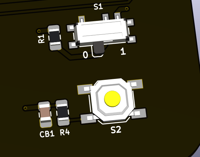
Figure 24 . Implementation of the vanilla reset circuit using an SPDT switch.
On these boards, to flash the MCU, the user changes the SPDT to position one and presses the push button, forcing the MCU to DFU. After the MCU is flashed, the user changes the SPDT back to the 0 position and presses the button again.
On BluePill boards, this is done through a simple jumper selector.
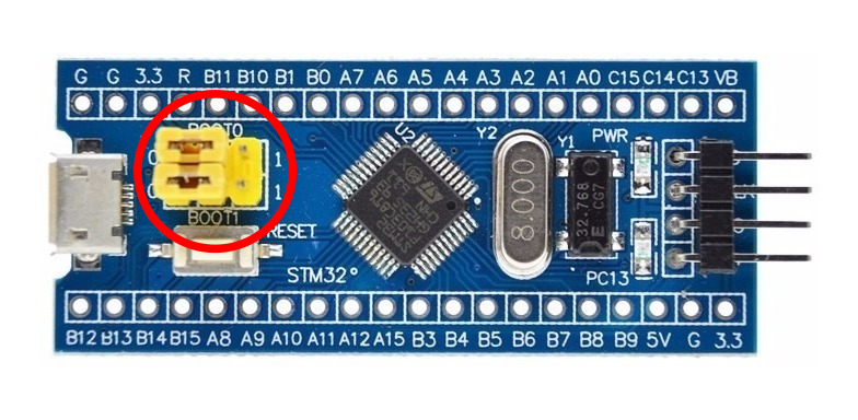
Figure 25 . Implementation of the vanilla reset circuit using a jumper selector in BluePill featherboards.
The vanilla circuit of Figure 23 can be modified just a little bit to make it more reliable, by addding a 100R resistor in series with the nRST button to avoid fast voltage changes in its capacitor and adding a little 100n capacitor to BOOT0 to avoid any fast transients, since it is a CMOS-type input.

Figure 26 . Slight modification from the vanilla reset circuit recommended by ST.
The problem of this vanilla circuit is that it requires way too many operations from the user. Turn SPDT to high, push button, flash, turn SPDT back to low, push button again. This can confuse some people and, ultimately, can make the flashing experience hard for people not tech-savvy.
(2) A new reset circuit
In middle development of the SharkPCB, a user by the name of ishtob blessed me with a piece of his knowledge and shared a reset circuit he was working on. A version of this circuit is depicted in Figure 27.

Figure 27 . ishtob’s original reset circuit for STM32.
The circuit is pretty clever; the idea is that the user will need to interact with the PCB only once to get it to work. When the push button is presset, the transistor will drive nRST to ground immediately; the reset and capacitor by BOOT0 will store voltage. By the time the user lets go of the button, BOOT0 is charged up and nRST is low. The MCU then goes into bootloader mode.
There are two caveats with this circuit. The first is that the diode is absolutely needed; without it, the charged voltage across the BOOT0 capacitor can maintain the transistor conducting and the MCU will not reset before BOOT0 loses its voltage to resistor decay. The second is that the transistor used has to have a base resistor, or else the base and emitter will be shorted – a bipolar transistor is basically two diodes back-to-back – and the circuit will never work; using a pre-biased transistor (also known as digital transistor) like the DTC123JK helps to keep component count lower due to the integrated resistors.
One might point out that this circuit only does half the job – it is able to get the MCU into DFU, but not able to reset the program. Well, as it turns out, resetting the MCU is not needed per se. See, QMK has software reset capabilities, so once the MCU is flashed it automatically resets. The user is also able to reset the MCU through a key combination, making use of the Boot Magic features of QMK.
The circuit works wonders. It is fairly simple, does the job and requires few components; revisions Alpha of the SharkPCB and ArcticPCB use it. Still, it is not good practice to rely solely on software reset and, as it turns out, it can be pretty catastrophic because locking the hardware reset can brick the MCU by getting it into a buggy state where software reset does not respond.
(2.1) Improving over ishtob’s circuit
In order to add a reset-and-DFU capability to the circuit, I had to turn my eyes to the BOOT0 branch. The nRST branch was pretty much figured out, so what I had to do was invent a way to modulate wether BOOT0 will be low or high at the time instant the user releases the push button, which is when nRST gets back to one and the BOOT0 pin is sampled and the boot option decided.
What I did was simple, yet complex. The addittion of a resistor between the diode and the BOOT0 branch will enable the RC circuit of BOOT0 to act as a timed charge RC circuit which voltage rises across time as the push button is maintained pressed.

Figure 28 .Improvement over ishtob’s original reset circuit.
Hence, the idea here is that the MCU boot option will be determined by how much time the user keeps the push button pressed. If for a short amount of time, the BOOT0 RC circuit will not have time to charge up enough to be considered high and the MCU will simply reset. If the button is held long enough, then BOOT0 will charge enough voltage to be considered high and the MCU will enter DFU.
The form and charge/decay rates of the BOOT0 pin are given by the R1, R2 and C1 components. The bigger the R2 over R1 proportion, the faster the circuit charges and the bigger will be the steady-state voltage. The higher the capacitance, the slower the voltage charges. The challenge then becomes to finely tune the values so that the times needed are convenient. For instance, if the charge is too fast, the user will not be able to press and release the circuit fast enough to reset it, and the MCU will always bootload. If the charge is too slow, then the user will need to keep the button pressed for too long a time.
To determine the exact times, first we need to know the logig level thresholds of the BOOT0 pin. In the MCU datasheet [3] one can see the following table:

Figure 29 .Datasheet table of minimum and maximum voltage logic level thresholds.
The table shows that using a feeding voltage of 3.3b, BOOT0 is considered low for voltages lower than \(0.3\times 3.3 - 0.3 = 0.69V\) and high for voltages higher than \(0.2\times 3.3 + 0.95 = 1.61V\). The circuit of Figure 28 was simulated usin LTSpice XVII; the simulation results are detailed below.
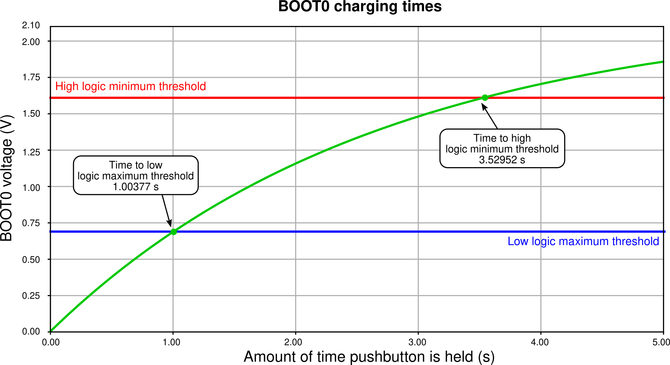
Figure 30 .Time simulation of the circuit in Figure 28.
The simulation shows that as the button is kept pressed, the voltage of BOOT0 crosses the low logic level maximum threshold at approximately 1 second and the high logic level minimum threshold at approximately 3.5 seconds. In other words, if the button is kept pressed for shorter than a second, the MCU will reset and, if kept pressed more then 3.5 seconds, the MCU will enter DFU mode. There is no telling what happens in between the 1s and 3.5s, as the logic level interpretation is not certain in that voltage zone.
(2.2) Considering components tolerances
There is, however, an inherent flaw wih the design of the Figure 28 circuit: the components used have tolerances which have to be accounted for; since these tolerances are considerable, the press timings will change with the real component values.
Let us define that the resistors have a 5% tolerance and capacitors have a 20% tolerance. First of all, since the nRST branch of the circuit is just pulling nRST to the ground and very fast, there is not much analysis to do with component tolerances here. The real problem lies with the RC charginf circuit of BOOT0.
Consider then the three comparison cases:
- Nominal case. All components are at their nominal values;
- “Slow” case. C1 and R1 are at their highest possible value of 120µF and 34.65kΩ and R2 is at its lowest of 95kΩ; hence this variation is the one that takes the longest to charge;
- “Fast” case. Pretty much the opposite of the slow case: C1 and R1 are at the lowest values 80µF and 31.35kΩ and R1 is at its highest 105kΩ, which is the fastest charging possible variation.

Figure 31 .Time simulation of the circuit in Figure 28 considering component tolerance-added “slow” and “fast” cases.
Figure 31 shows the simulation of the three cases. The simulations show that the fastest time the circuit will cross the low logic levle maximum threshold is at approximately 0.75s, while the longest time the circuit will take to cross the high logic level minimum voltage is approximately 4.5 seconds. This means that by using the circuit of Figure 28, if the user presses the button for no more than 0.75 seconds the MCU is guaranteed to reset, and if he or she presses the button for longer than 4.5 seconds the MCU is guaranteed to DFU.
These times are, however, not to my liking. As can be seen in Figure 31, the spread of timings between the curves is way too high. In order to solve that, I changed the tolerances of the resistors to 1% and the tolerance of the capacitor to 5%.
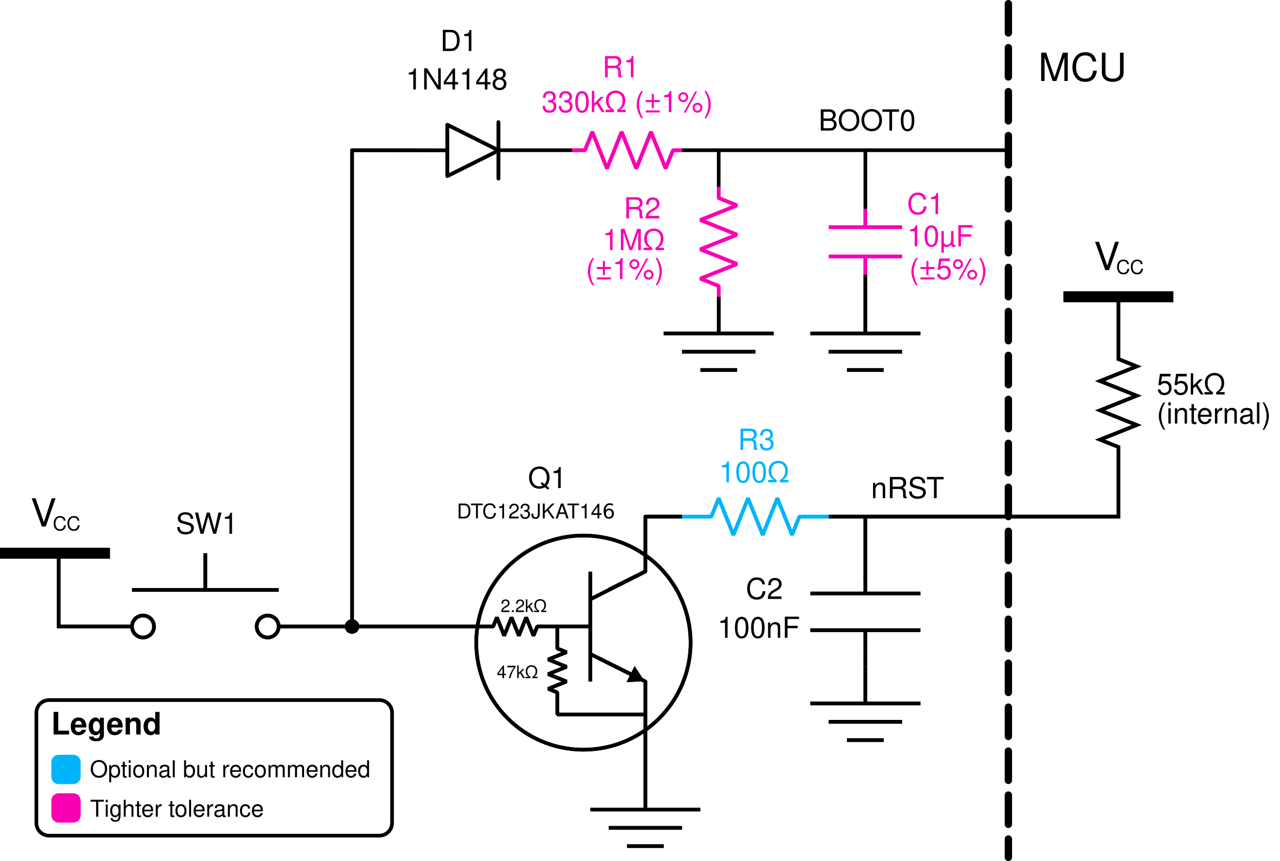
Figure 32 .Improved reset circuit with tighter tolerances.
Figure 33 shows the simulation of the same circuit with the tighter tolerances, which is much, much better: now the needed times for guaranteed low and high levels are 0.94 seconds (which can be considered 1s for a human reaction time) and 3.8 seconds.
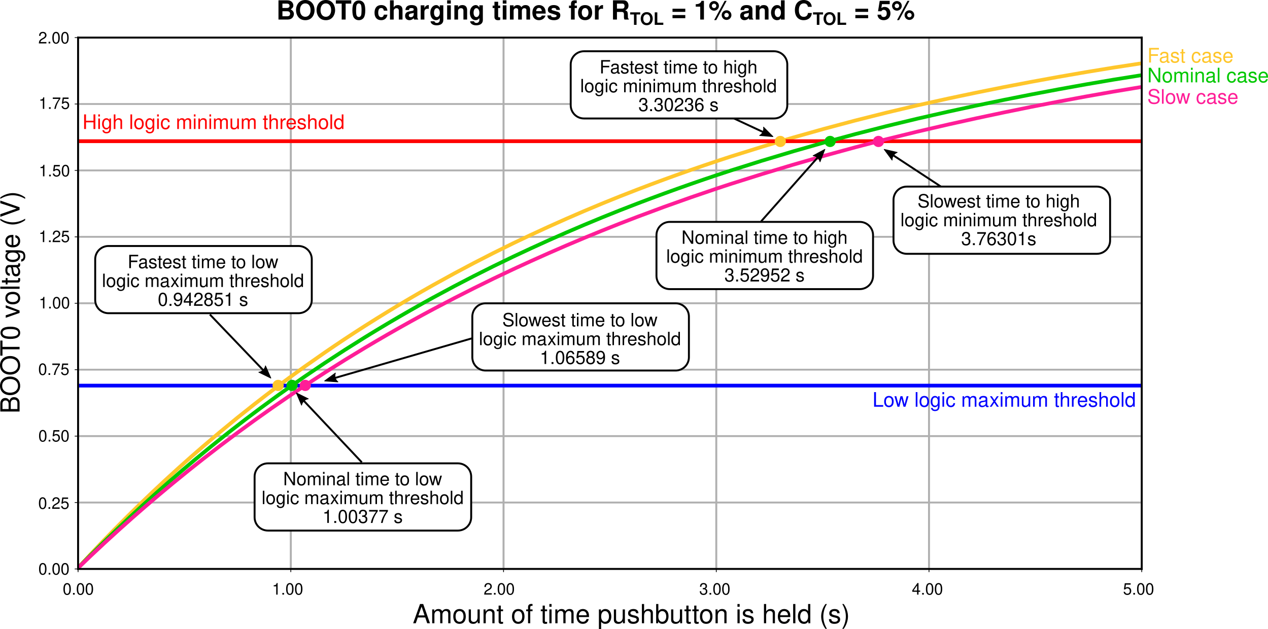
Figure 33 .Time simulation of the circuit in Figure 32 which has tighter component tolerances.
The choice of tighter or normal components is really a designer choice, but I highly recommend the use of this tighter circuit since the price raise is really not much (maybe a dollar?) and the circuit becomes much, much more reliable.
(3) Handling the discharge issue
(3.1) Describing the discharge issue
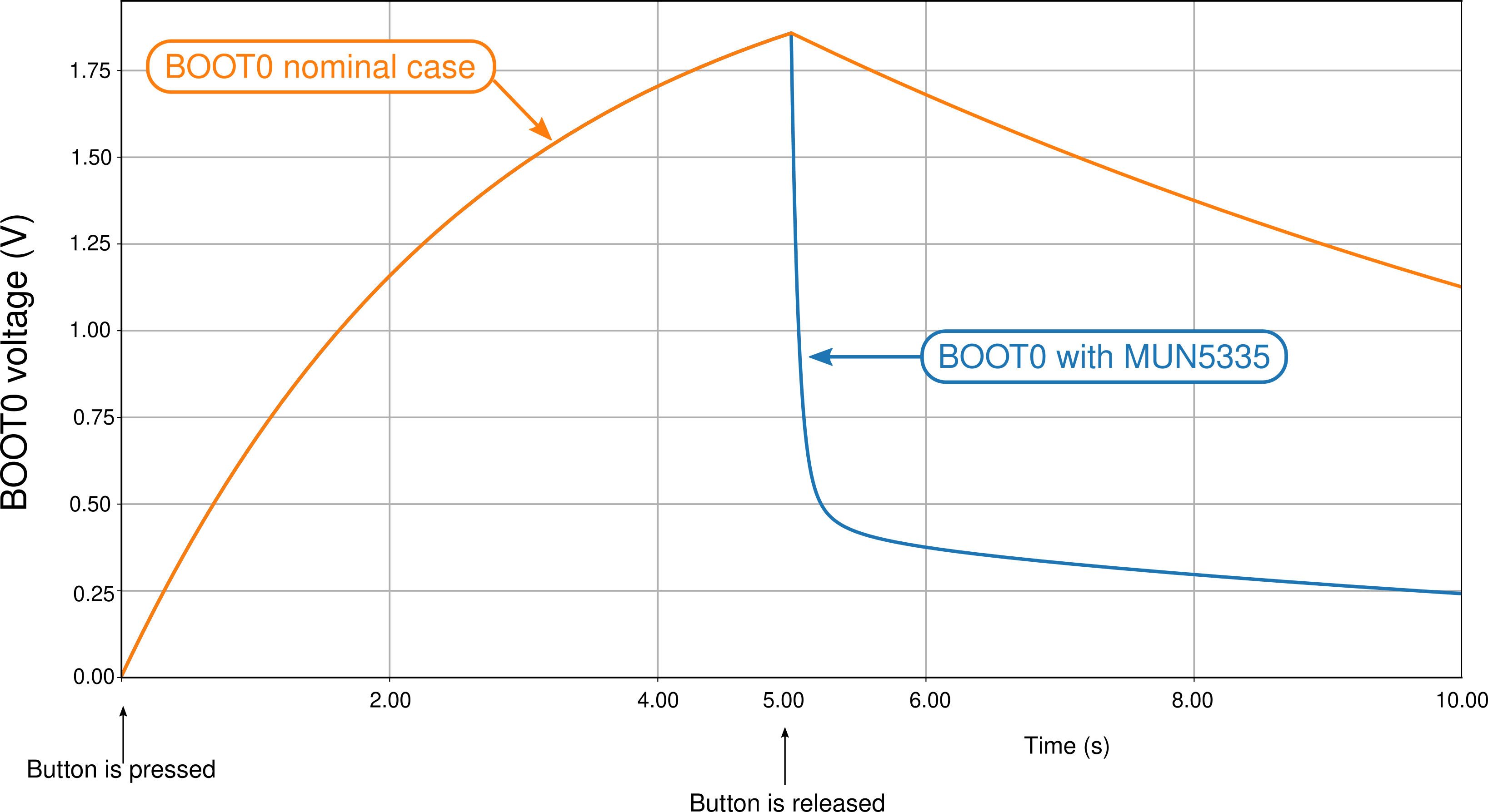
The circuit of Figure 28 still has an issue: the discharge of the BOOT0 circuit. The charging of the circuit sure does serve our purpose, but what happens after the MCU has reset or entered DFU mode? Of course, the BOOT0 circuit discharges – the energy charged in the C1 capacitor makes its way to ground with R2. However, the discharge rate of this circuit is way too slow.
Figure 34 shows thhe simulation of the reset circuit during and after the push button is pressed. This simulation shows that, after the button is released, the BOOT0 takes 10 seconds to fall back to the low logic level threshold. Picture the following situation: the user holds the button and gets the MCU into DFU mode, only to realize that that was not the intention, they wanted really only to reset the circuit. Well, now they give the button a fast press and, surprise: the MCU still goes to DFU when the user didnt hold the button. Since the BOOT0 pin was charged, they must now wait 20 seconds to press again.
A vendor might see the disaster this situation can become: the user now thinks they have a faulty PCB and proceed to rage on the vendor website about how the PCB does not work as intended and they want a refund.

Figure 34 .Simulation of the reset circuit of Figure 28 during and after the pushbutton is pressed.
(3.2) Using the MUN533
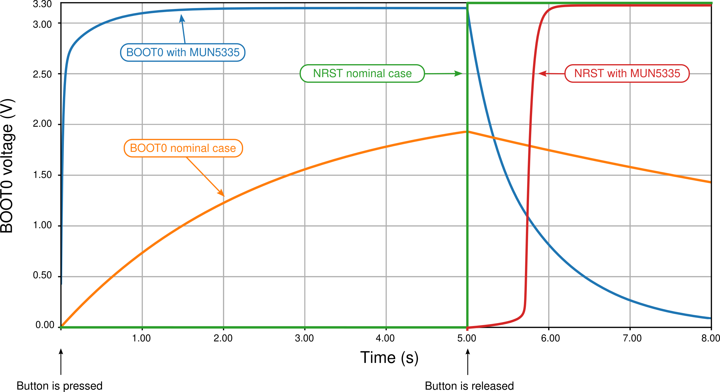
In order to fast discharge the BOOT0 pin, an additional PNP transistor is used, generating the circuit in Figure 35 . The use of the MUN5335DW1T1G integrated circuit makes it possible to integrate both the pre-biased NPN transistor for the nRST pin as well as the PNP transistor for the BOOT0 discharge in the same SOT-23-6 package, keeping component count the same as the old circuit without the discharge.
The idea here is that when the push button is relased, the PNP transistor will conduct and drive BOOT0 immediately to zero, therefore dis-charging the BOOT0 pin and making it possible to re-activate the circuit.

Figure 35 .Yet another improvement over the reset circuit, this time with a discharge transistor to ensure voltage fallback discharge.
Figure 36 shows the BOOT0 and NRST voltages as the push button is pressed and released. The keen reader will however be able to find the issue with this circuit: the added PNP transistor does what it was supposed to; the BOOT0 pin with the MUN component indeed discharges way faster than without it. However, the addition of this PNP transistor also comes with the addition of two transistors that bias it, both internal to the MUN device.
These transistors have two detrimental effects.
- First, the 47k resistor and the 2.3k act in parallel with the 33k resistor, making a much lower parallel resistance and interfering with the charge pattern of the BOOT0 pin in such a way that it charges way faster than the nominal case, making it impossible for the user to release the button before BOOT0 is charged, effectively removing the circuit’s capability to reset the MCU;
- Second, the internal PNP resistors also make a path that bypasses the D1 diode which was supposed to keep the BOOT0 from maintaining the base of the NPN transistor charged. With this new path, the voltage and the NPN base is maintained, causing the NRST voltage to not rise immediately, but takes near a second more to rise again.
(3.3) Using the UMF5N
The apparent solution to this problem would be to adopt a PNP transistor that does not integrate the biasing resistors. ROHM Semiconductors’ UMF5N is a device which houses a pre-biased NPN and a non-biased PNP, that is, a NPN that has the internal transistors but a PNP that does not.
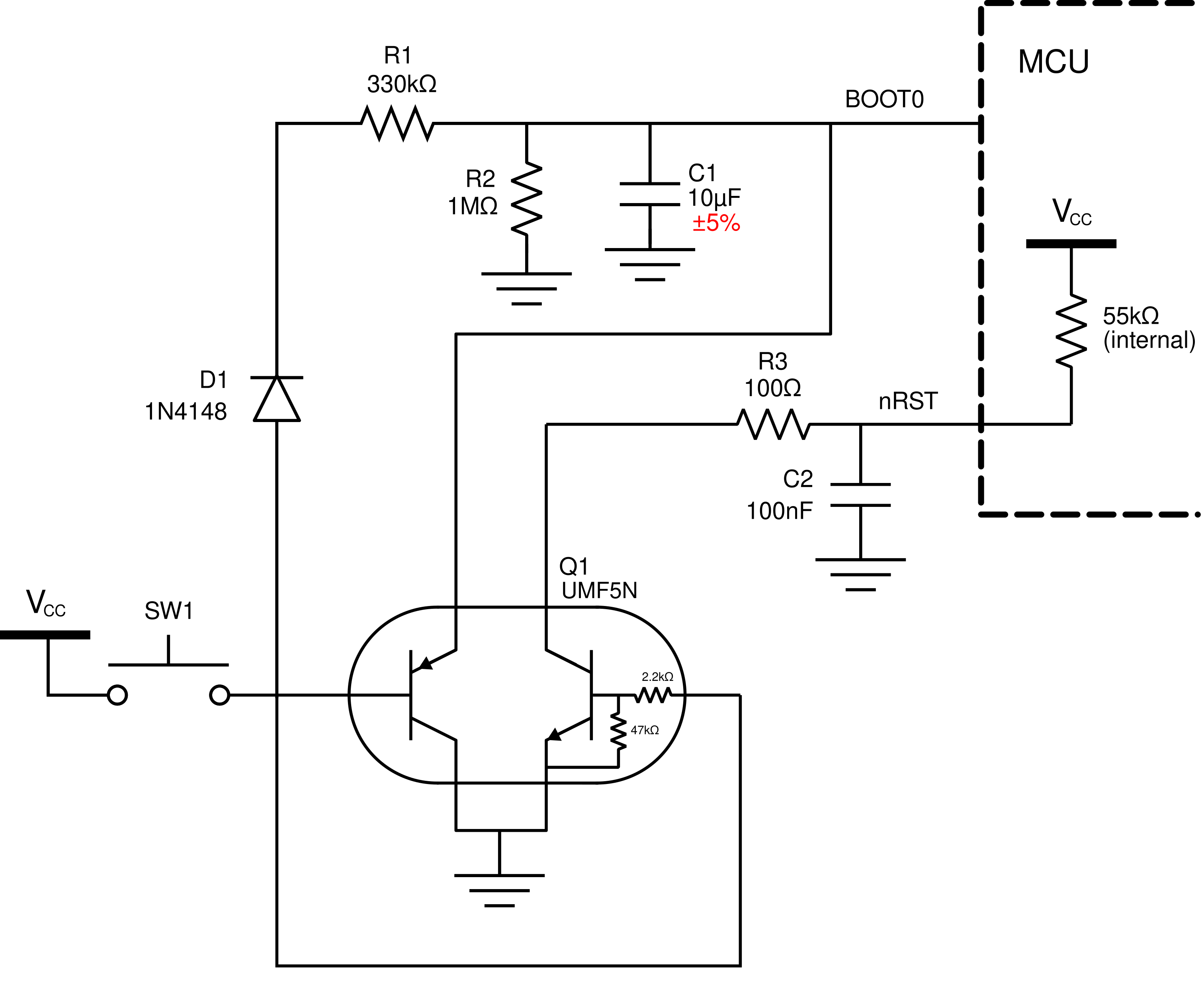
Figure 37 .PNP-discharged circuit of Figure 35 using the UMF5N, which contains a non-biased PNP transistor.
The Figure 38 shows the time simulation of the circuit. Since the UMF5N does not have the biasing resistors, hence does not make a current path that bypasses the diode D1, the charging profile of BOOT0 is kept the same as the nominal case. The PNP transistor does the job of discharging the circuit much faster than the nominal case, and the NRST voltage rises as fast as the nominal case.
(3.4) using a jfet
I still was not quite happy with how the UMF5N device solves the issue. As can be seen from the simulation in Figure 38, the BOOT0 voltage does fall profusely in the first seconds after the push button is released, but adter some time it still looks like it holds some voltage (approximately 0.3V). That is due to the bipolar transistor’s circuit characteristics. In simple terms, a bipolar transistor is fundamentally two diodes constructed back-to-back; this means the bipoalr transistor has an exponential characteristic such that the lower the base voltage, the collector current is diminished exponentially. After a while, when the BOOT0 circuit is already discharged, the PNP transistor cannot conduct current fast enough to make the BOOT0 discharge completely to zero volts.
The solution I found was to use a JFET transistor, which are known to be unparalleled analog switches. The circuit with the JFET as an analog discharge switch is shown in Figure 39.
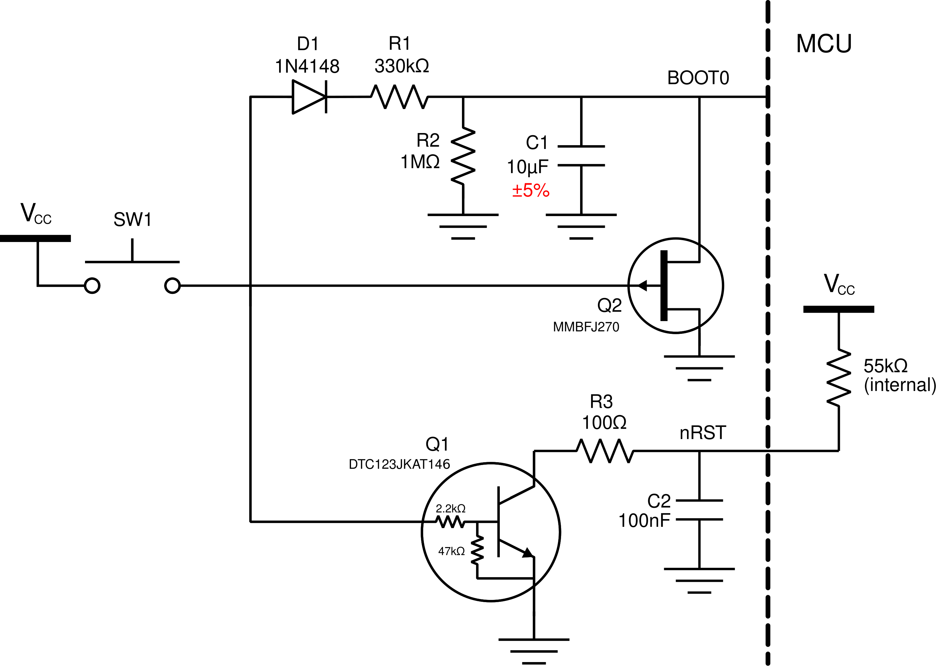
Figure 39 .Schematic of the discharged-reset circuit using a J270 JFET instead of a bipolar transistor for the BOOT0 discarge.
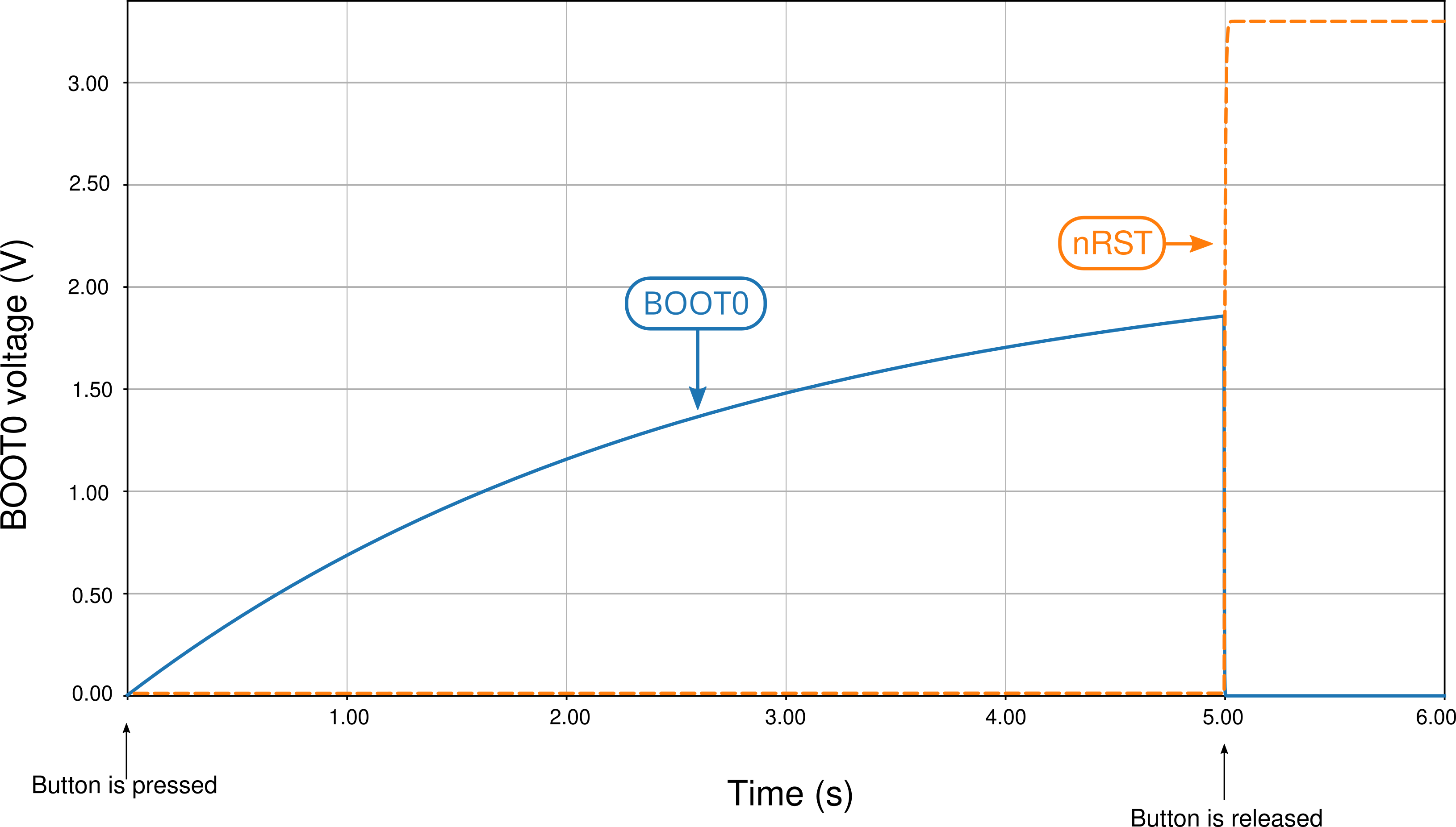
Figure 40 .Time simulation of the circuit in Figure 39 during a 5 second press of the push buttom and release, showing BOOT0 and nRST pins voltages.
As the simulation shows, the JFET does the job perfectly: it instantly grounds BOOT0, discharging it immediately. The problem now is… it does the job way too well. Figure 41 shows the zoomed-in version of the plot in Figure 40. The plot shows that the JFET discharges BOOT0 so fast that the pin reaches its low threshole even before nRST reaches its high, meaning that the when the MCU samples BOOT0 – after nRST has reached high logic – BOOT0 will already be at low state. This means that the circuit will never go into DFU mode, only reset to flash!

(3.5) JFET reset with delayed discharge
To delay the JFET discharge time, all that is needed is to add a resistor to the JFET, as shown in Figure 42. The time simulation of this circuit to a press, hold and release of the push button is shown in Figure 43.
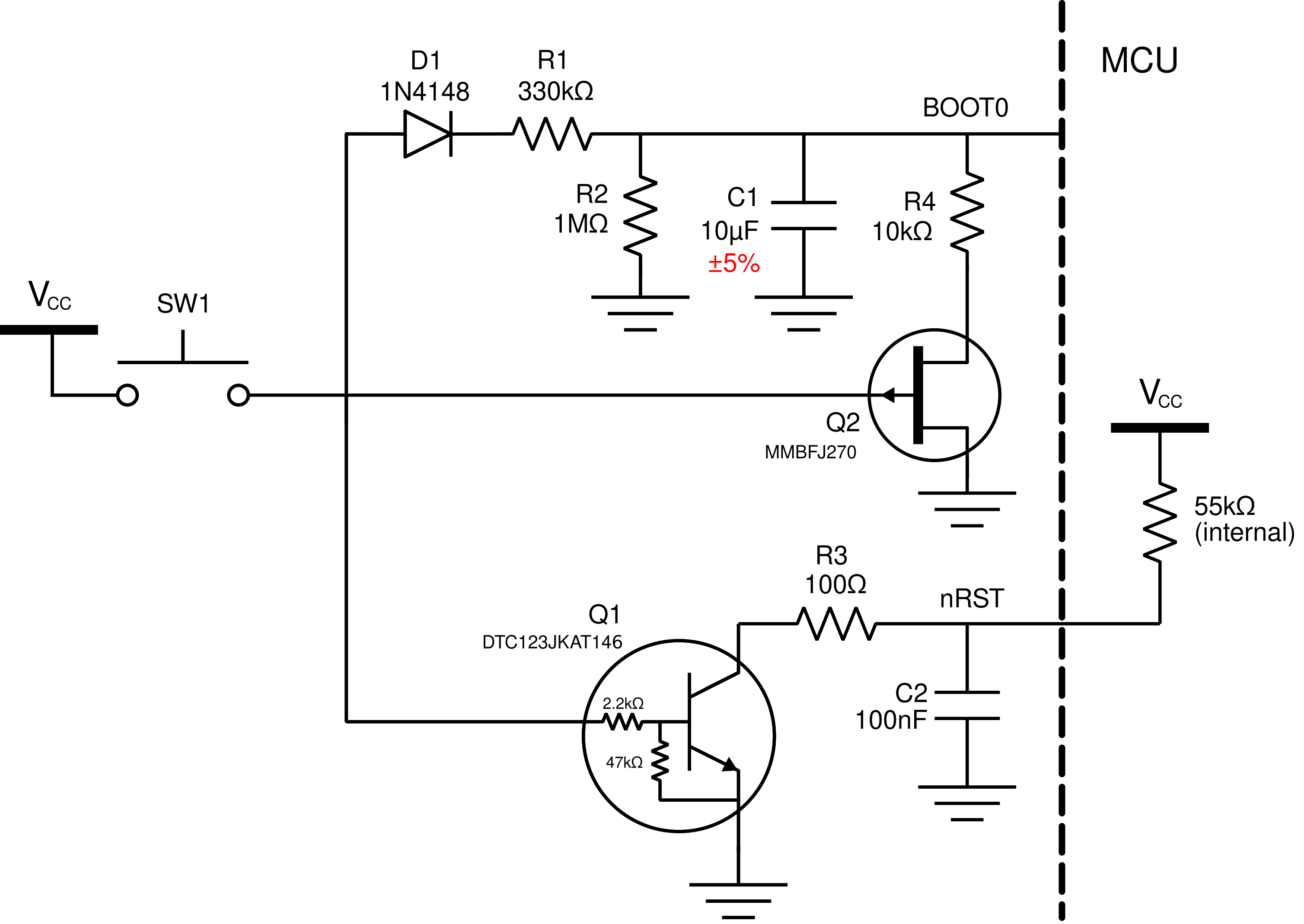
Figure 42 .Schematic of the reset circuit using a delayed-discharge JFET mechanism.
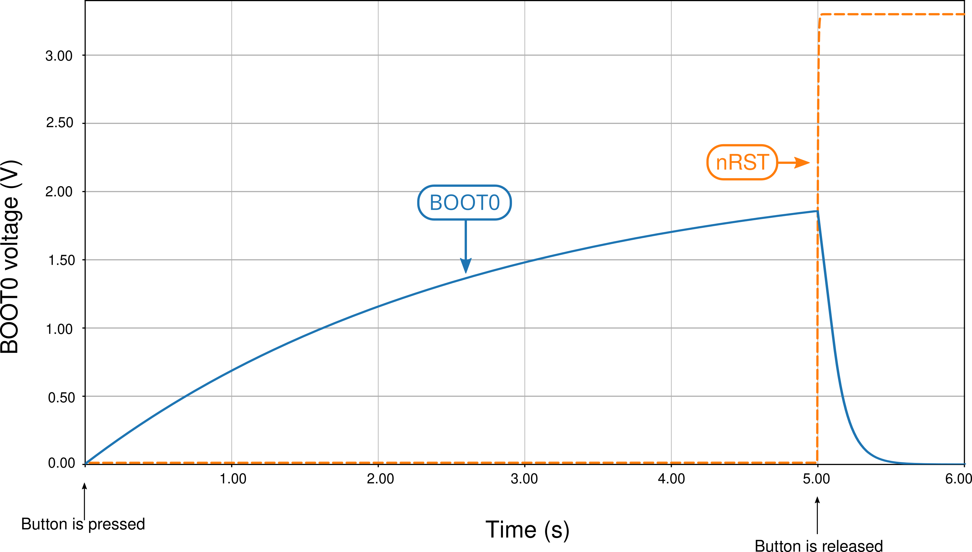
Figure 43 .Time simulation of the delayed-discharge JFET mechanism circuit of Figure 42.
This circuit is simple but ingenious. What is happening here is quite sophisticated yet so simple. The JFET acts as a switch that commutes the BOOT0 RC circuit charge and discharge, as seen in Figure 44.

Figure 44 .Simplification of the schematic of the reset circuit using a delayed-discharge JFET mechanism showing the JFET as a discharge resistor switch.
When the push button is pressed and the BOOT0 circuit is charging, the JFET does not conduct current and the 1MΩ resistor is used to charge the circuit slowly, abiding by the designed cross times we seen before; as a matter of fact, the JFET conducts so little current that the 10kΩ resistor is almost non-existant. When the push button is released, the JFET starts conducting current and the 10kΩ resistor is shorted to ground, making a parallel resistance with the 1MΩ. Since the former is so much smaller than the latter, the resulting parallel resistance is very close to 10kΩ.
So at the end the JFET acts as a switch that commutes the resistors; when the push button is pressed, the circuit charges with the bigger 1MΩ and hence charges slowly. When the button is released the circuit “changes” the RC resistance to 10kΩ, which makes it discharge swiftly.
The 10kΩ value was not chosen randomly. It was chosen to be much smaller than 1MΩ, bringing the charge/discharge commutation effect yes, but it was also chosen such that the discharge of the JFET was delayed in such a way that the nRST pin would have time to reach high logic before BOOT0 completely discharged. Figure 45 shows the time plot of the time simulation of the delayed-discharge JFET circuit with a 10kΩ resistor.

Figure 45 .Simplification of the schematic of the reset circuit using a delayed-discharge JFET mechanism showing the JFET as a discharge resistor switch.
As the plot shows, the delayed discharge allows the circuit an approximate 25 milisecond time between nRST reaching high logic and BOOT0 discharging to the high logic threshold, which is far more than enough. Remember that, according to the datasheet, the BOOT0 pin is sampled on the fourth rise of the clock signal of the MCU once nRST is high; since the MCU works at 72 megahertz, a 25 milisecond time is very reasonable.
Finally, as far as the R4 value goes, almost any value between 2kΩ and 10kΩ will give a plausible result. The next plot shows a simulation of the falltime of BOOT0 on the circuit given several values of R4, ranging from 0 to 10kΩ in 1kΩ steps. Naturally, the bigger the R4 value, the slower the discharge is and the more available time the MCU has to sample BOOT0 at high time.

Figure 46 .Simplification of the schematic of the reset circuit using a delayed-discharge JFET mechanism showing the JFET as a discharge resistor switch.
Figure 47 shows a parametric plot of the available time that the MCU has to sample BOOT0 as high level, that is, the time difference between the instant nRST voltage rises to its high logic level threshold and the time instant BOOT0 voltage falls back to its high logic threshold, as a function of the R4 resistance. As we seen before, at 0kΩ, the available time is negative, that is, BOOT0 falls below high logic level before nRST hits its high logic level. This is counterbalanced at approximately 1kΩ (1.021kΩ to be more precise) where the available time is zero, that is, BOOT0 and nRST hit their high level thresholds at the same time. At 2kΩ the available time is 2.8559 miliseconds – enough on its own. The reason I chose 10kΩ is because it gives a very nice headroom to work with component tolerances and is a good value to find with tighter tolerances.
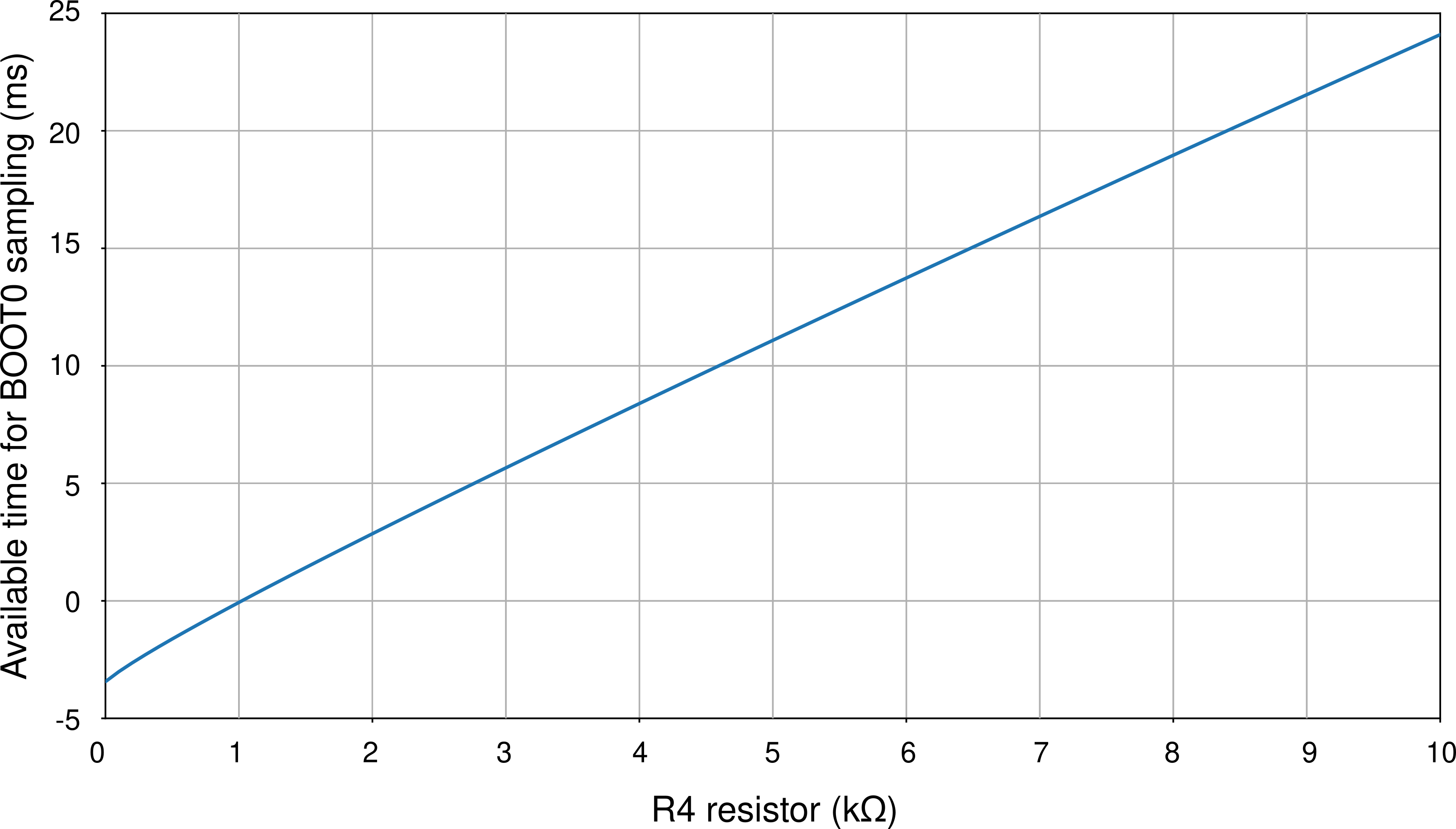
Figure 47 . Parametric plot showing the available time the MCU has to sample a high logic level BOOT0 once nRST is sampled high as a function of the discharge resistor R4.
(5) Conclusion
The article presents the development and simulation of various possible reset circuits, of which three are viable, meaning they can reliably drive the MCU both to reset and to DFU mode. Figure 48 shows these reset circuits.

Figure 48 . Final list of the viable developed reset circuits developed: the “vanilla” circuit recommended by STM, the “improved reset” and the JFET “delayed-discharge reset circuit”.
(5.1) Which circuit should I use?
Confronted with so many possibilities one might ask which is the best or which should they use. Although I do not know if there is a “better” or “worse” circuit, there are adtanvages and disadvatages with every single one of them:
- The “vanilla reset” circuit is by far the simplest one. It is the most reliable and simple to implement and requires few simple components. However, the fact that it requires a rather complicated routine to flash and reset makes it non-ideal for user usability; reestated, the fact that it is not single-action and requires several steps to work may be a problem in troubleshoot and operation for the common non-experienced users;
- The “improved reset” circuit is the initial implementation of the BOOT0 charging machanism where a short button press is a reset and a long button press drives the MCU to DFU mode. It is fairly complicated and requires precision 1% resistors and a 5% tolerance capacitor on the BOOT0 circuit to be reliable, but delivers the single-action proposal of this article with cheap and simple enough components. The problem here being that each activation of this circuit should be approximately 30 seconds apart, due to the fact that the BOOT0 circuit takes time to discharge;
- The “delayed discharge” circuit is the most user-friendly but is the most sophisticated and requires fancy components like the J270 JFET (that costs up to 20 cents a piece) and the special tolerance resistors and capacitors. The fact that the delayed discharge is performed means that the circuit is immediately discharged after button release, meaning the user can press the button rapidly and the circuit will work every time without problems, delivering the promise of a “truly single” action.
The usage of each circuit is of course at the discretion of the designer; my personal experience and opinion is that the vanilla circuit is fine for prototyping reasons or if the PCB you are designing is a personal project and not intended for mass production and selling. If the objective is user friendliness and mass selling, I definitely recommend using the JFET delayed discharge circuit. For 20 cents more you get a reliable single-action circuit that works as intended every time, as opposed to the “improved reset” that, albeit being single-action, can be misused if the user is not patient enough to wait 30 seconds for each action or is simply ignorant of its functioning. It is my opinion that a product should not be designed while supposing that the user knows its inner workings, hence why I recommend the delayed-discharge circuit.
(5.2) Tighter tolerance components
Another possible question that arises is: are the tighter tolerance components on the BOOT0 charge circuit really needed? The true answer is no. The time plot of Figure 31 shows that it’s perfectly possible to reset and DFU the MCU without the special tighter tolerance components. The real only thing that changes from a circuit that uses common-tolerance components and a circuit that uses tighter tolerance components is simply the guaranteed times needed. For instance, with normal tolerances, the MCU is guaranteed to reset if the button is released under 0.7 seconds after being pressed and guaranteed to DFU is the button is held for at least 4.6 seconds.
The usage of tighter component tolerances gives you two advantages.
First, that the times tom reset and DFU are a little bit more reasonable – to reset release under a second of press and to DFU hold for at least 3.8 seconds. The curse of the exponential growth characteristic of the charging circuit means that if you try to make the reset timing larger – to a second, for instance – the DFU timing will also be much longer; if you try to make the DFU timing shorter, the reset timing will be much shorter. This means that, with common tolerances, it is very difficult to adjust the reset and DFU timings because trying to adjust one will exponentially (literally) affect the other. With tighter tolerances, however, the change is still exponential; but since the parameter uncertainty is that much smaller, the effect is not that great.
To illustrate this advantage, imagine a common serial RC circuit with a constant voltage source \(V_S\). Then the charge timing of the capacitor voltage is given by
Hence, the time \(T\) the capacitor takes to reach a voltage \(V\) os given by
Imagine now that \(R\) and \(C\) vary with uncertainties \(\Delta R\) and \(\Delta C\), that is,
Call \(T_0\) the nominal time to reach voltage \(V\), that is, the capacitor would reach that voltage if the components were perfect:
Then through the propagation of uncertainty formulas, the uncertainty of \(T\), that is, \(\Delta T\), is given by
The keen reader might indetify this as a elliptic parabolloid in the \(\Delta T\), \(\Delta R\) and \(\Delta C\) variables. This means that the time uncertainty \(\Delta T\) grow parabolically with the resistor and capacitor uncertainties, which goes to show that the time uncertainty is very, very sensible to these quantities.
The interested reader might also calculate the partial derivatives of the sensibilities of \(\Delta T\) with respect to \(\Delta R\) and \(\Delta C\), which will prove the parabolic growth of the sensibility.
If the reader is still incredulous, let us calculate the time sensibility in the terms of this last formula. If we are using common tolerances, that is,
Then the normalized time uncertainty equals 20.62%. If the tighter tolerances are used, that is,
Then the time uncertainty equals 5.10%.
These calculations motivate the second advantage that this circuit gives you; this advantage is deeper and less visible, but much more important: reliability. Suppose that you are using the circuit with common tolerances in a 1000-unit production run. Since every PCB has different capacitanca and resistance values, each PCB has a different time charging curve; what I can guarantee is that this curve is at all times located between the “fast case” yellow curve and the “slow case” pink curve of figure Figure 31, and that the charging times between PCBs will vary in a 20.62% margin. This means that the actual timings to reser and DFU can vary wildly between PCBs. On the other hand, if you use tighter tolerances, the charging curve will be confined between the fast and slow curves of figure Figure 33, which are much closer together; hence the actual timings of each PCB will vary mildly (inside a 5.1% margin, which is much more tolerable), as opposed to the large variations you would get if you used the more common tolerances. The fact that the circuit is more predictable and less variable – hence, more reliable – means that the behavior of the circuit will be more uniform across all production units, that is, while the normal tolerance components will give each unit a very different timing, the tighter tolerance will make sure all PCB units will be under a very strict margin. This, in turn, makes sure that your product is much closer to specifications.
My opinion and experience on this matter are this: use component footprints so that the common tolerance and the tighter tolerance components share the same footprints; for instance, use a 1206 resistor and a 0805 capacitor footprint, as there are both 5% and 1% 1206 resistors just like 20% and 5% 0805 capacitors. That way you can keep prototype costs down by using the more common tolerances and, on the final more polished product, you use the tighter tolerances components because, at a large scale, the price per PCB will be increased marginally while the circuit will be much more reliable and user-friendly.
References
| [1] | STM32F0x1/STM32F0x2/STM32F0x8 advanced ARM-based 32-bit MCUs series reference manual. Available at this link. Last accessed june 22, 2020. |
| [2] | (1, 2) Getting started with STM32F0x1/x2/x8 hardware development. Available at this link. Last accessed june 22, 2020. |
| [3] | STM32F072xB / STM32F072x8 MCUs datasheet. Available at this link. Last accessed june 22, 2020. |