PCBWay sponsorship: how to review PCBs
Back in october of 2019, I received an e-mail from a representative of PCBWay. They wanted to sponsor some components of the Acheron Project by offering me free prototyping PCBs in exchange for a review video and an article. You can see the video in this link and this is the article. In this text I will detail my thought process of reviewing a PCB manufacturer, and review the quality of the PCBs that PCBWay sent me and how my past experiences with PCBWay.
The review is done by six parameters I have and pictures of what I mean. I will compare these PCBs to one PCB I have from JLCPCB, which is largely and largely and generally used as a budget PCB manufacturer, and point out the differences between a higher-price, higher-quality PCB and a middle-quality, budget-price PCB.
About PCBWay
Of course, PCBWay would not sponsor the project without my counterpart: introducing them and their website, how they operate and how you can use their services.
PCBWay is a big player in the business of Printed Circuit Board (PCB) manufacture (F) and assembly (A), which we generally abbreviate as PCBFA. This is also called full-turnkey process. You can hire their services at their website, where they have an Instant Quote process. This means that you can submit your files to their webiste and receive an immediate quotation of the price you will pay for their services, if you use PCBF only. If you want to hire PCBFA, they will analyse and review your project and make a quotation for the PCBs, the components and their services, assigning to you a sales representative and sending you a very detailed quotation within a week.
For everyone interested in using their services, always have in mind that they are based in Asia (China I believe), so if you are thinking of importing their PCBs to sell, most countries will apply importation tarrifs. However, their price is almost always worth it over local manufacturers.
Why accepting sponsorships
At a first glance one might ask himself why should I accept a sponsorhip from a big PCB manufacturer.
First, because hardware development takes money. Much money. Sometimes more than what I can pay, actually; a round of five PCB prototypes will cost easily from 130 to 180 US dollars. In general, my modus operandi is that I don’t charge for a PCB project but the person that wants the PCB pays for prototypes.
This works well for some kind of keyboards; high-end keyboards like the Austin and the Elongate, which have a nice catering audience and can easily be sold in a group-buy, generally don’t present cost issues when it comes to prototyping because the GB runner knows his idea will get paid. However, some layouts, like the most common universal 60%, will be difficult to get prototyping money for because there are so many universal 60%s out there, so making a new one is really seen as unnecessary. However, every keyboard designer worth his salt should design one of those; in general, I even recommend for aspiring PCB designers to start with that layout becaue it really offers all the issues and possibilities a keyboard PCB will have.
In this sense, I negotiated with PCBWay so that they sponsored three projects of mine: the ArcticPCB, the KeebsPCB and the Acheron Ruler. These projects were also chosen because they are very close to my heart.
Another good reason to accept sponsorships from PCBWay is because through their sponsorship I can give the community a quality PCB design without charging anyone for it.
How I review PCBs
The PCB reviewing process is not straightforward because it sometimes takes too much time to complete. The final test of a PCB really is when you solder the components in and test all the features. However, there are some preemtive ways to assert the quality of a PCB before you have to solder all components in.
Another issue of reviewing PCBs is that there is also a heavy aesthetical factor to it; in the enthusiast communities, the appearance of the PCBs is very important to the customers because the PCB is an integral part of the project, specially in keyboards and audiophile equipments. Issue with this being that aesthetics are a very subjective matter; however, there still is some objectiveness to it. For example, if the PCBs are heavily scuffed or scratched like Figure 1 and Figure 2 below, that is simply unacceptable.
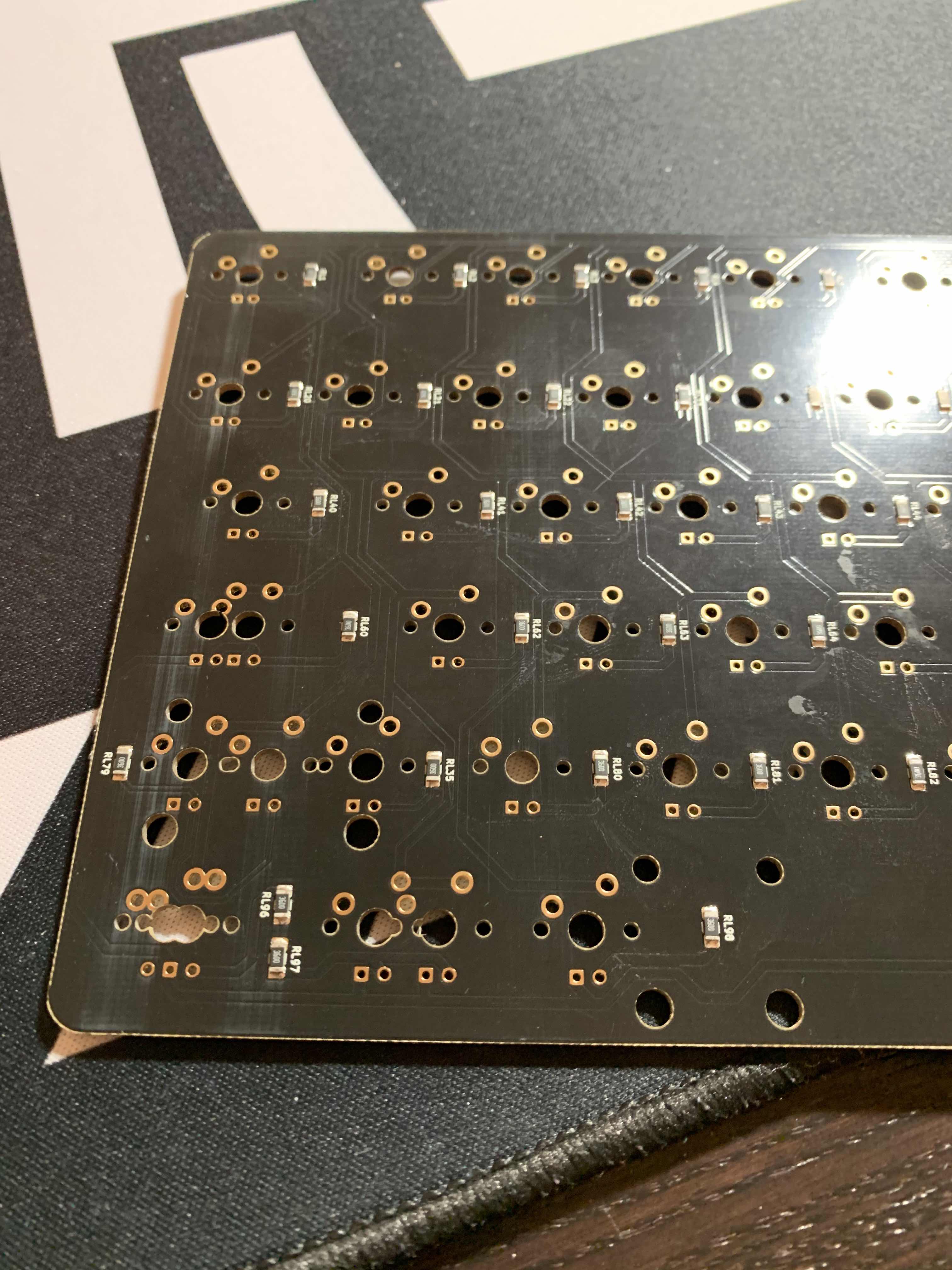
Figure 1 . First picture of a heavily scoffed and dirty PCB. This should serve as an example of a objectively bad aesthetics and innaceptable state of a PCB.
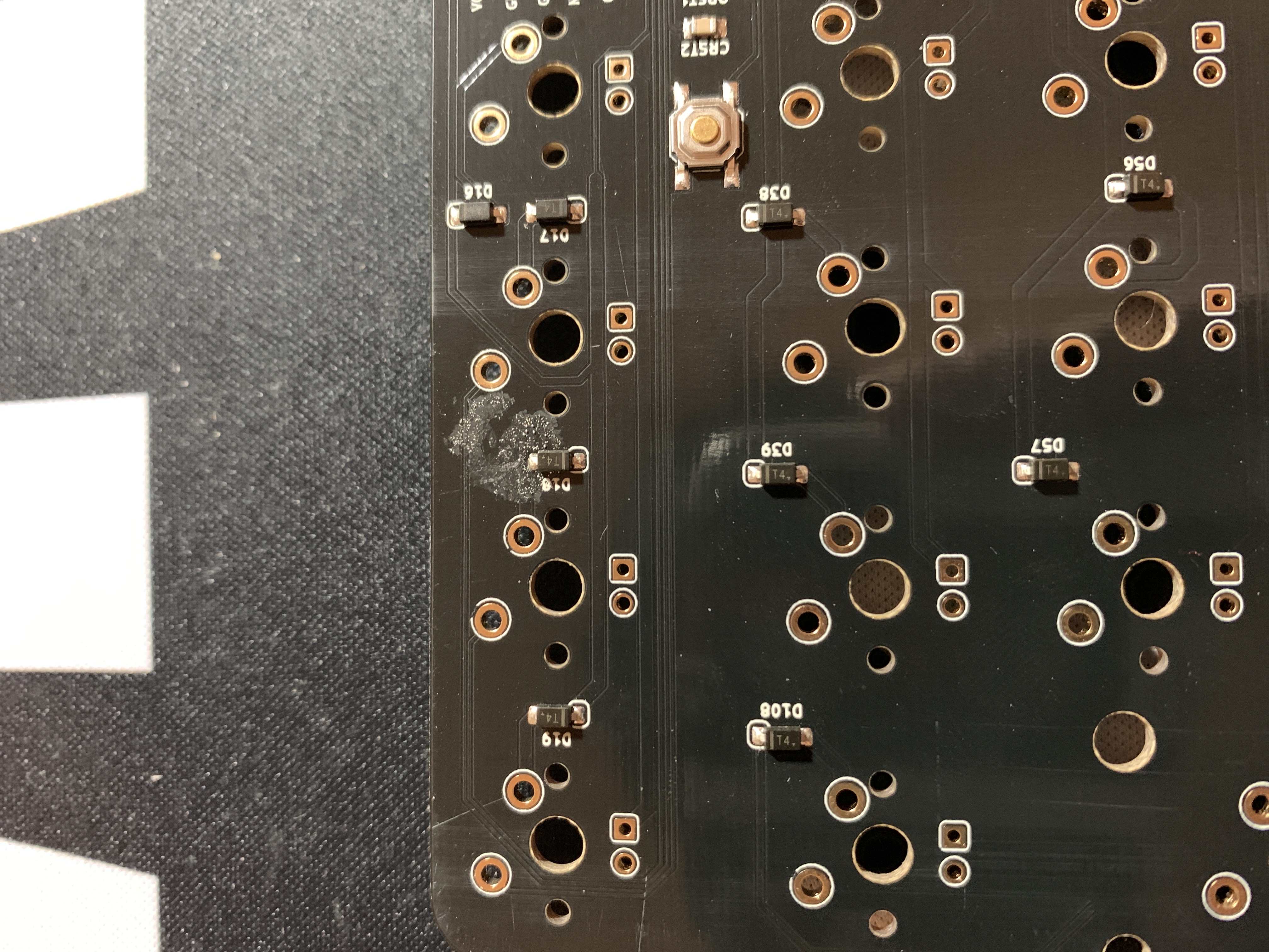
Figure 2 . Second picture of a heavily scoffed and dirty PCB. Note that, beyond the scoffs, there is a weird stain around diode D18, which is most probably a result of a badly used solderpaste or flux, since we can see flux of tin on the stain.
The main parameters I use to review a PCB are:
- Silkscreen
- Soldermask;
- Soldering pads and their metallization;
- CNC machining of the PCB edges, castellated holes;
- Overall aesthetics like color, appearance of the PCB;
- Customer support and representatives, and my experience with PCBWay.
One might also ask why “price” is not on this list. This is because since the PCB manufacture and assembly market has many big players, prices are very competitive and will not change between the many competitors. Also, the majority of these competitors offer Instant Quotes, meaning that you can submit your files toi their website and receive a quotation immediately. You can use this feature to easily compare the prices among the competitors.
There is, however, an outliner in this process. Most famouly, JLCPCB, which is known to make cheap PCBs at low quantities, ideal for prototyping. in this article I’ll also show a PCB that I have from JLC and how does a budget PCB compare to a high-quality, more expensive PCB.
Hence the following chapters will, each by each, focus on these five parameters. They were analysed in photographic detail, and pictures will be presented.
1. Silkscreen
Over the years I have used many PCB manufacturers, and one thing that I particularly like about PCBWay is that they have one of the cleanest silkscreens I know. This is specially important in SMD PCBs because since surface components are generally very small, having clear silkscreen is important for the soldering process and the prototyping, as well as maintenance whenever you need to replace a component.

Figure 3 . Some of the silkscreen markings on the ArcticPCB prototype. Note how every single character is recognizable by the naked eye, even most of them having 25 mil (~0.6mm) height.
Figure 4 . Some of the silkscreen markings on the KeebsPCB prototype.
Figure 5 . Some of the silkscreen markings on the Acheron Ruler prototype.
Both prototypes show very clean and readable silkscreen characters, even in a very small character height of 25mil. This is very desirable and makes everything better.
Clean silkscreen is also good for those nice graphics and logo you might want your PCB to have.

Figure 6 . Silkscreen logo of the Acheron Project on the ArcticPCB.

Figure 7 . Silkscreen OSH logo on the KeebsPCB.
To contrast with these, below is an image of the SharkPCB prototype version pre-Alpha manufactured by JLCPCB.
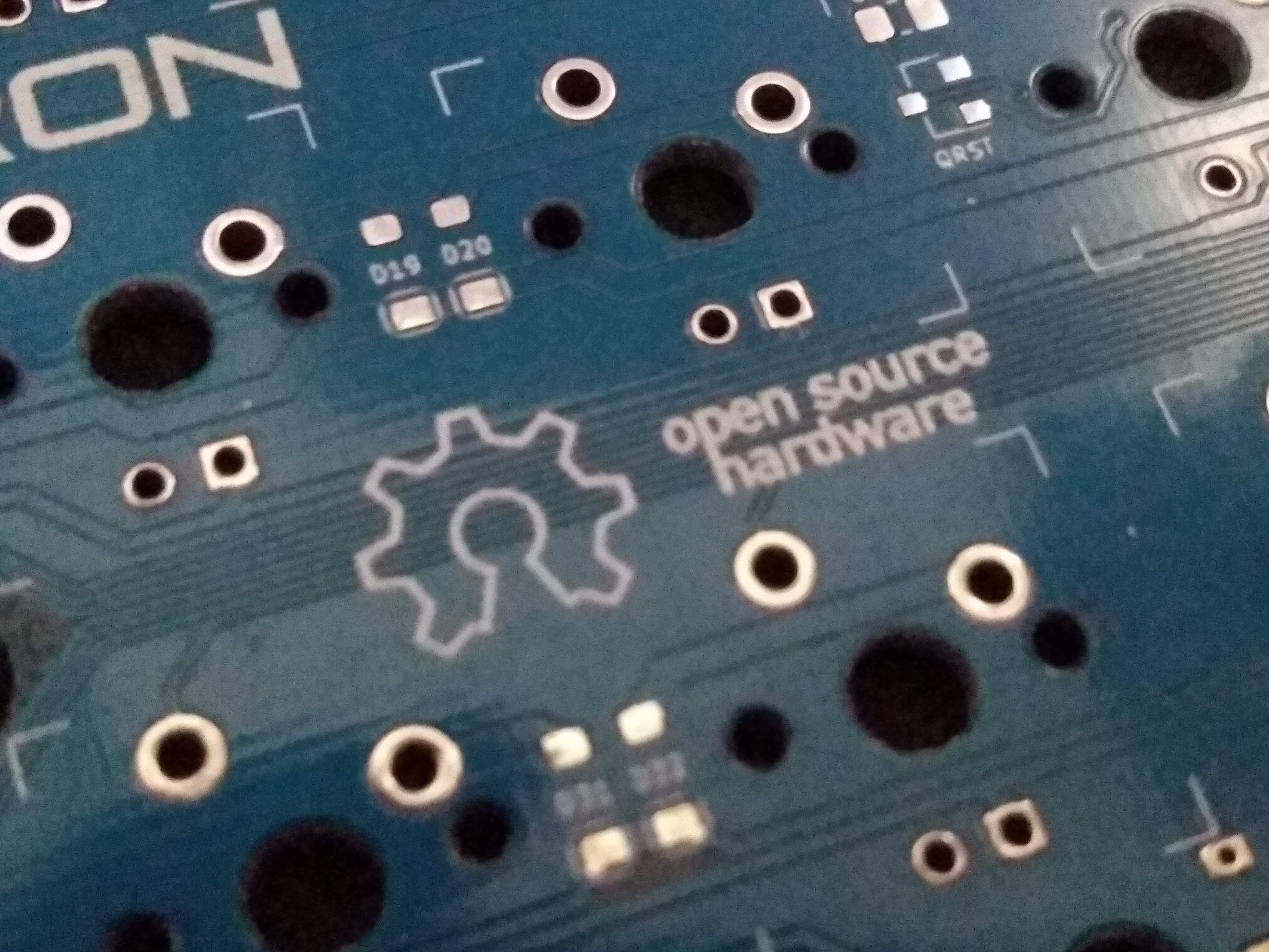
Figure 8 . Silkscreen OSH logo on the SharkPCB prototype.
It becomes very clear how in JLCPCB’s case the silkscreen markings are not so clear and “fuzzy”. Also note how the characters are much harder to read and spot.
It is important to note that in some cases the silkscreen can be incomplete or misaligned, as in Figure 9. This is indicative of a very lazy production process and for a final product is not torelable.
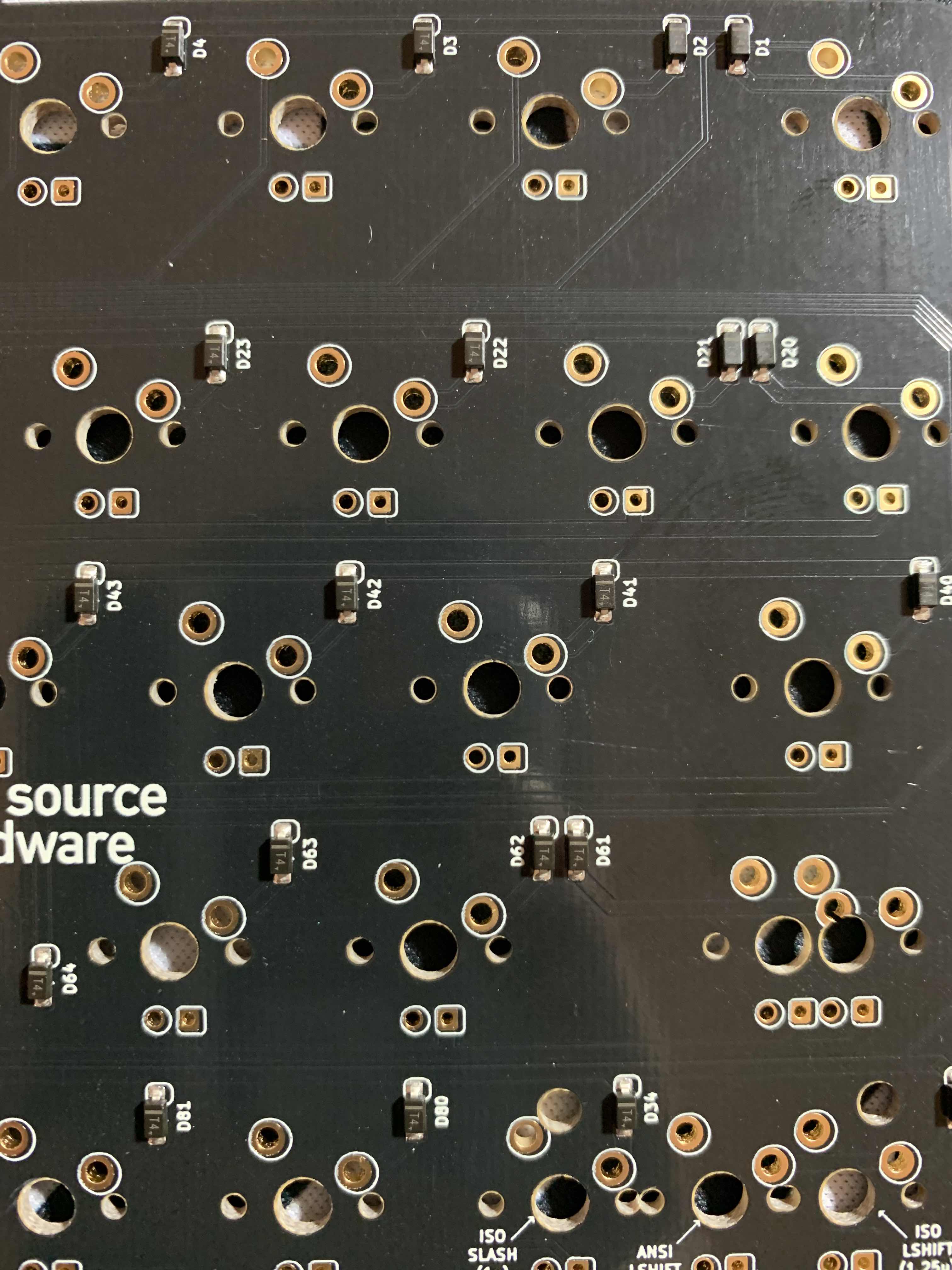
Figure 9 . Picture showing a case od misaligned silkscreen.
2. Soldermask
The main way to look at soldermask is coverage and uniformity. Soldermask is basically a protective cover to avoid exposing the PCB copper and unintended shortcuts. Its main purpose, however, is to repel solder so that the tin sticks only to the metallic pads it is supposed to. It also has a very aesthetic function, as it is basically what gives the PCB its color.
Having a soldermask not cover any part of the PCB means it can present oxidation and unintended shorcircuits. Having it uneven or not uniform means that it can wear off in some time or with bad handling.
A good stress test is to try scraping the soldermask off at some point in the PCB; ideally, a soldermask should be very difficult to wear or scrape off, so taking a blunt and a sharp object and trying to rip soldermask off the PCB in various places is the way to do it. Another way to detect bad uniformity is putting the PCB against a light source and checking for color differences.
In the video I forgot to add a section where I try to scrape the soldermask off, so I will only say that the soldermask was fairly strong and difficult to remove. I had to apply a good amount of pressure to remove the soldermask, even when using a sharp object.
Figure 10 . Full picture of the ArcticPCB showing coverage and uniformity of the soldermask.
Figure 11 . Silkscreen OSH logo on the SharkPCB prototype.
Just like the silkscreen, the soldermaks can too be incomplete or misaligned, like in Figure 12. This is very detrimental to the PCB as misalignments in the soldermask can prevent it from doing its work, that is, avoiding solder bridges and wrong solders.
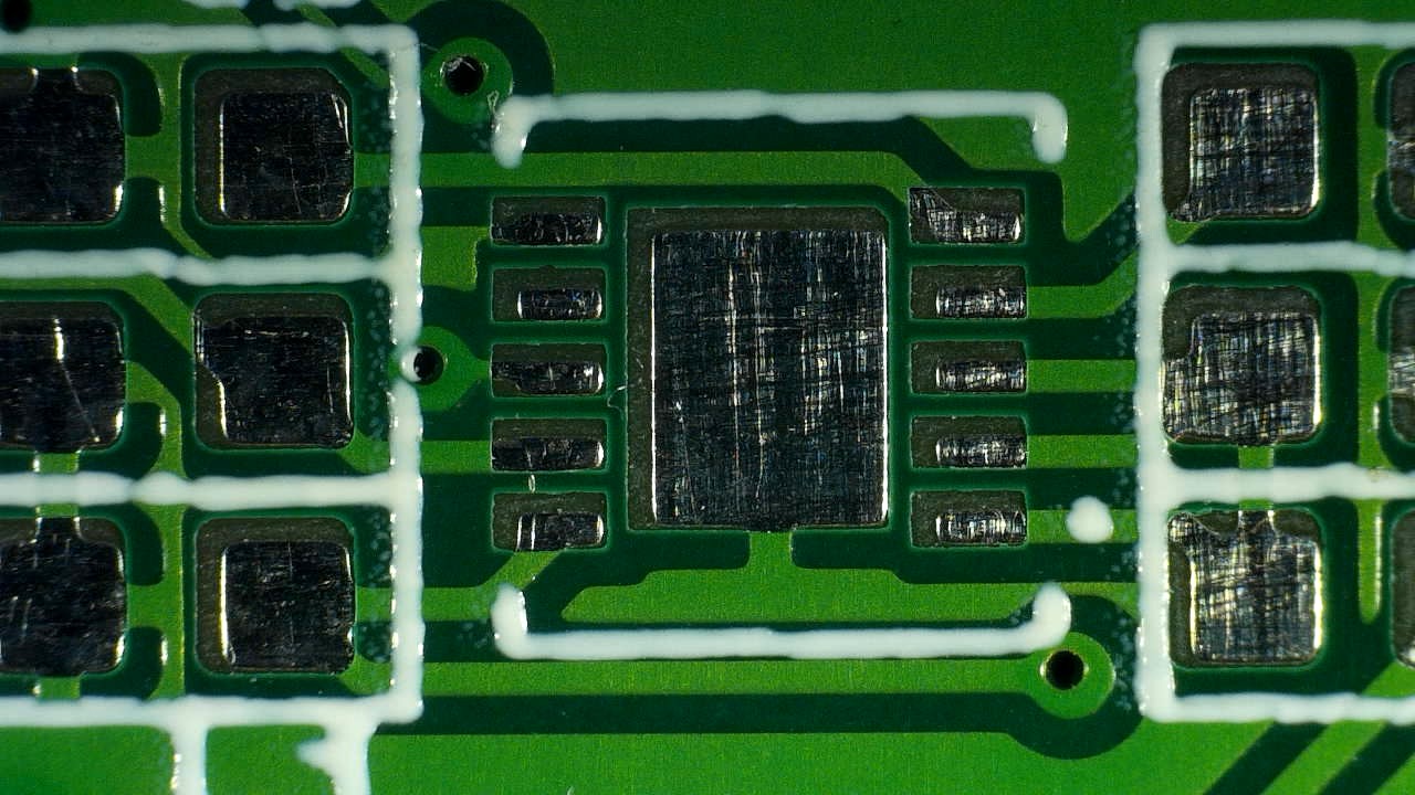
Figure 12 . Picture showing a case of misaligned soldermask, Courtesy of Discord user @xyz .
3. Soldering pads and metallization
In general, the most important part of a PCB are the soldering pads, because that is where the components will be soldered and the contact points between components and traces are the very purpose of a PCB.
It needs to be said that the quality of the surface finishing of the pads depends highly on the technology used. There are three main surface finishes that most PCB manufacturers offer, the frst and cheapest of them being HASL (Hot-Air Solder Leveling), where the PCB is dipped into a bath of molten solder in and the excess is removed by hot air knives (a stream of high intensity, high pressure and hot temperature stream of laminarly flown air). HASL however tends not to hold the best results because the excess solder tin does not come off easily, even with air knives, leaving uneven and inconsistent surfaces. It also is not good for fine-pitch PCBs and compex PCBs, as it can very easily generate solder bridges. HASL also has the issue of generally using leaded solder; there are, however, lead-free HASL options.
The second most available copper finish is Organic Solderability Preserving, or OSP, which consists of coating the PCB with an organic material that bonds to the copper, preventing it from oxidation, until the actual soldering. The organic compounds are generally the heterociclyc azoles, which due to the nitrogen in their chain form coordination bonds with the copper atoms, producing nitro-copper-heterocycle complexes. This finish is sometimes regarded as the most “environment-friendly”. OSP has a very nice simple process and flat surface, while also being very price-effective; its main issue being it has a very low shelf life because the organic compounds are not oxigen-stable and degrade over time. Also, the coating is not metallic, so it is very sensitive to bad maintenance and handling.
PCB factories will also offer ENIG (Electroless Nickel-Immersed Gold). Over the exposed copper a layer of nickel is deposited through an auto-catalysed reaction and, over it, a layer of gold (yes, real gold!) through electrodeposition. This is by far the finish that gives the most quality feel and looks, because it leaves a near-perfect surface due to the very even layer of nickel. It also offer excellent oxidation process, as gold does not oxidate in the presence of oxigen. Moreover, ENIG is ideal for applications where an exposed metal surface is needed, e.g., common membrane switches.
Finally, some PCB factories can offer IAg or Silver Immersion copper finish. This finish is not easily found and is used only for very specific applications, specially those where high-speed designs are concerned because silver, being the most conductive metal known to man, offers very low high frequency signal loss due to skin effect, enhancing signal integrity in the PCB. The issue with IAg is that silver is notably prone to oxidation, taking a blackened shade.
Personally I recommend going HASL for prototypes, since they don’t need to be very aesthetically pleasing or high-quality; they just need to work. That’s what you get with HASL, and that’s what I did with the protos PCBWay sent me. H1owever, if you are doing the final product to sell or distribute, I always go with ENIG, ensuring a nice experience for the PCB user.
As for reviewing, the best way to review the pads and metallization of a PCB is to have a big pad, like a logo or an inscription that exposes a big part of the PCB. This makes it easier to evaluate the finish. See Figure 13 and Figure 14 .
Figure 13 . Showing of the Arctic Logo to evaluate the metallic pads of the PCB.
The figure shows a large pad of the PCB. Since the PCBs were ordered with HASL, the finished is “waved” and clearly shows that the metallization is not surface-perfect. The next picture also shows that.

Figure 14 . Showing of the Acheron Logo on the Acheron Ruler to evaluate the metallization of the PCBs.
I must say that this is not the best metallization I have ever seen, but it is definitely usable and up there. Also that kind of waving and imperfections in the metallization is completely normal on HASL technology, and since what I see in these pictures is acceptable, I really can’t say PCBWay is at fault here. For comparison, Figure 15 and Figure 16 show the mmetallization of a ENIG board, also done in PCBWay.

Figure 15 . Showing of the DriftingMechanics logo on the AustinPCB. Note how the surface finish is much more smooth.
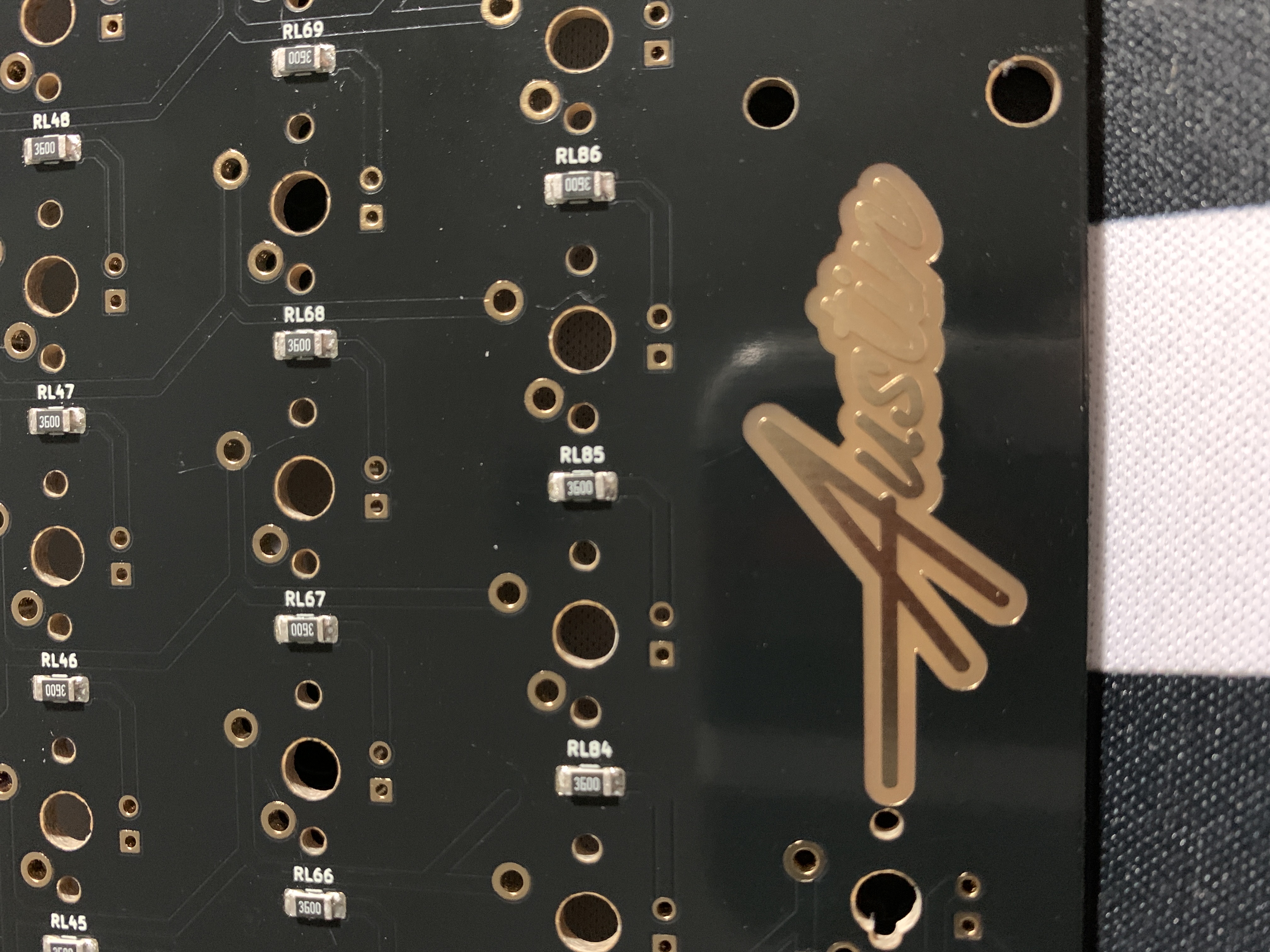
Figure 16 . Showing of the Austin log on the AustinPCB.
All in all, I find the pads in the PCBs I received from PCBWay very acceptable and workable; then again, not the best I have seen, but way up there. I have received some PCBs from factories where one or another pad was not completely covered, hindering it unusable because it was oxidized, meaning that the PCB was dirty or oily when submitted to the solder bath. Another PCB I received had way too much solder excess, meaning that probably the solder bath was too cold or the air knives were not pressurized or hot enough.
4. PCB edges and castellated holes
PCB edges are important because by evaluating how well that part was done tells us how precise the machines of the factory are. There are two main ways to evaluate drilling and edges on a PCB, the first being through holes that are near the edge and the second being the holes that literally cross the PCB edges, like castellated holes.
For instance, in both ArcticPCB and KeebsPCB, the backspace stabilizer holes are very near the PCB top edge, and the spacebar stabilizer holes also are. Figure 17 and Figure 18 show the backspace stab holes and the spacebar stab holes, respectively.

Figure 17 . Picture of the backspace holes on the ArcticPCB.
Figure 18 . Picture of the spacebar stab holes on the ArcticPCB.
Specially in Figure 17, it is interesting to note the quality of the edges and cuts, including the holes. Those two holes near the PCB edge, in the milling process, can be opened up and torn.
More importantly, however, is to note that the leftmost pad on the top is cut right in the middle by a hole; not only that, no barbs or burrs of metal lie on the holes. This usually happens and can cut fingers or take solder away from the pad.
This problem, however, manifests itself more apparently in castellated holes, which are plated holes on the edges of the PCBs. Figure Figure 19 shows one of the castellated holes of the ArcticPCB.
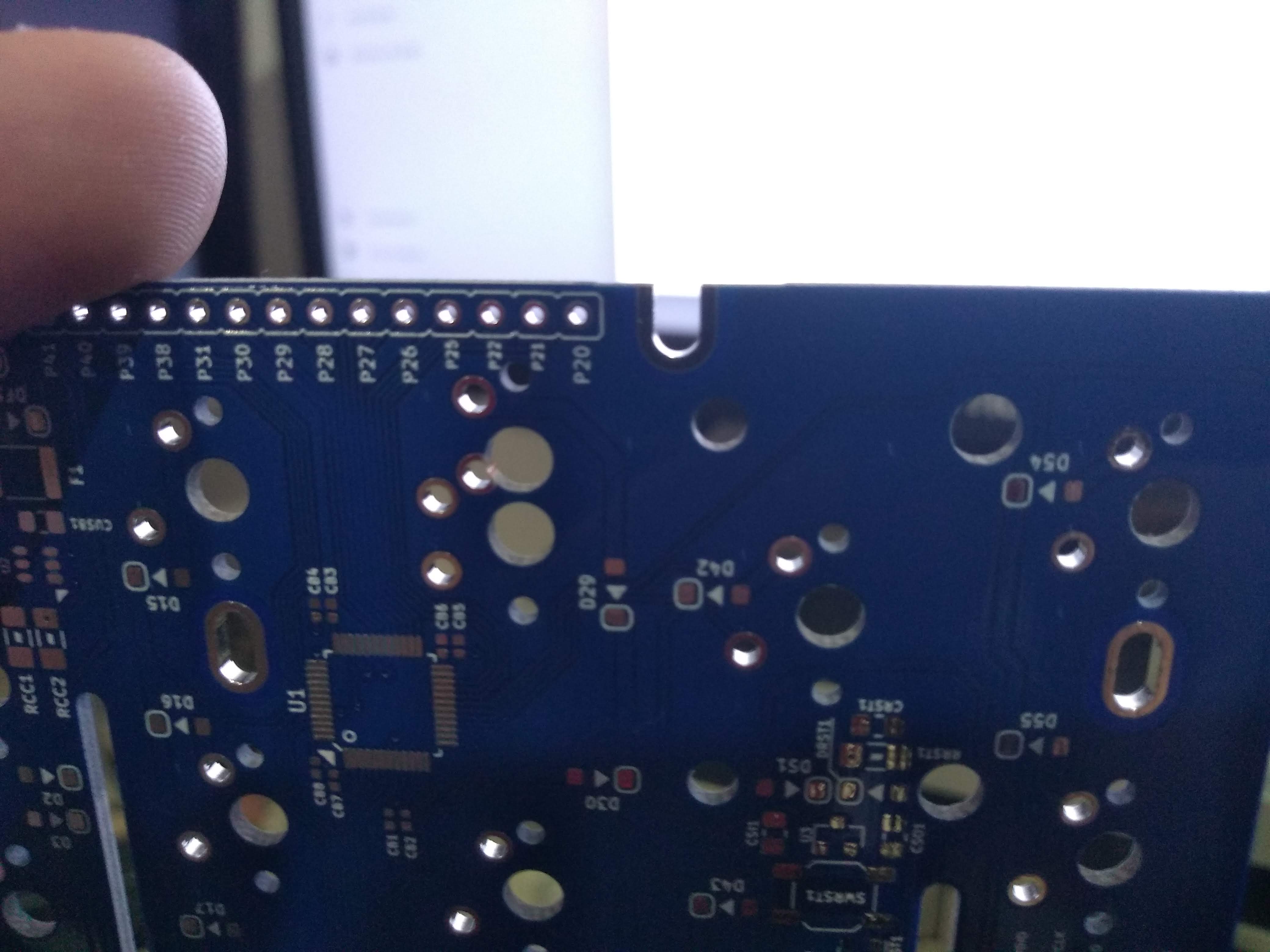
Figure 19 . Picture of one of the castellated holes of the ArcticPCB.
The picture shows that there are absolutely no problems with the castellated hole, and the plating is flawless; no burrs or flawed plating.
5. Overall aesthetics and appearance
This section is, again, very subjective and there are many ways to look at this. However, there are some objective patterns we can use.
First, the PCBs came with absolutely no scratches or scuffs, apart however from two PCBs that came a little bit scoffed. This happened – I believed – because the vacuum plastic that the PCBs were wrapped in was torn, so the vacuum went away and some PCBs grinded on one another. I feel strange to blame this on PCBWay, but one can speculate. First, the obvious choice is to blame this on the shipping companies, and that a rough shipping made the plastic tear. Another possibility would be that PCBWay did not wrap the PCBs properly. I will not make comments on this or assume one of both options.
I know that I am biased, but I find the PCBs very nice and appealing, especially because it is very clean and metallization looks great. Below are some images of particularly nice spots on the PCBs.
Figure 20 . Picture of the MrKeebs logo on the KeebsPCB.
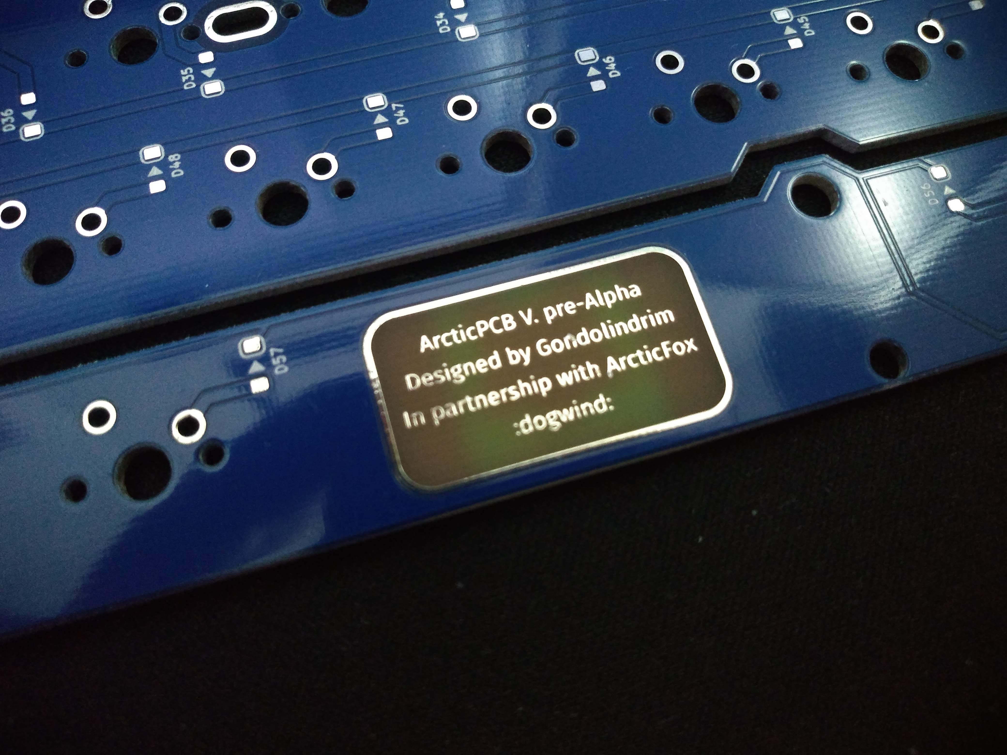
Figure 21 . Picture of the label on the ArcticPCB.
Also, aesthetics and feel are also affected by the quality of the edge cuts. Take a look at figure Figure 7 to note how a PCB from JLCPCB has very rough edges; I have seen cases in some PCBFs where the edges are so badly cut that they are sharp and cut fingers and hands.
6. Customer support and my experience
However technical, the PCB manufacturing is still a business and customer relations and support is a big part of the perception of the user.
My experience with PCBWay has always been very easy. They are always on point and direct; they also respond quickly and solve problems.
I had, however, one problem with PCBWay that brought some troubles. For a particular keyboard, the PCBs were ordered from them and a good portion of the PCBs came with very noticeable and deep scoffs and scratches. I immediately messaged PCBWay and they were fast to respond, sending new PCBs for free in a couple days. However, the new PCBs came scratched and scoffed too, so the vendor had to give every buyer a discount.
As of today – December 14, 2019 – we have not received yet new PCBs again, but this has been a huge turndown. Their support is still good and we are waiting on a response, but the issue is we have a deadline to consider in delivering the keyboard PCBs.
At the end, PCBWays customer service is still the best that I have dealt with but the way this situation has been handled is very problematic.
Once we see a closing to this issue I will write it here.
Conclusion
Can I recommend PCBWay? Depends.
The PCBs are good. Really good. Perhaps some of the best in the business. For the final selling products, I do recommend them. Their customer support is also very good and responsive, solving questions and issues fast. Whatever issues I had with them are still open, so they have time to redeem themselves.
However competitive they are in the PCBFA part, they have some real difficult quotes to meet at PCBF, specially when JLCPCB comes in play. Yes, JLC does not make as good PCBs and I wouldn’t sell them to a customer, but for prototyping there still is no beating their price. For prototypes the quality is very acceptable.
I recommend everyone to order and test the PCBWay services at least one tim e.
Then again, I feel very thankful and humble that PCBWay decided to sponsor these PCBs because without their support they wouldn’t be prototyped or would take much longer.